Zhiheng Xingsheng
PCB Assembly

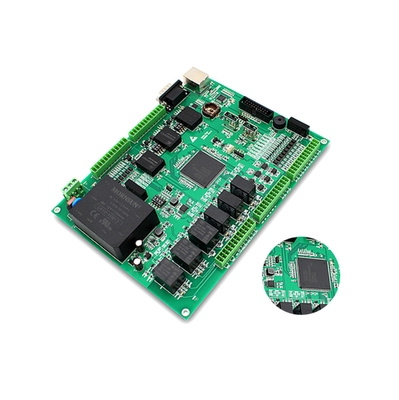
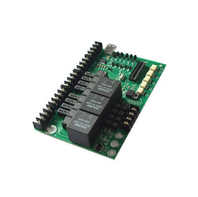
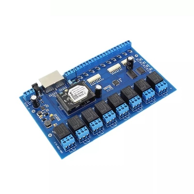
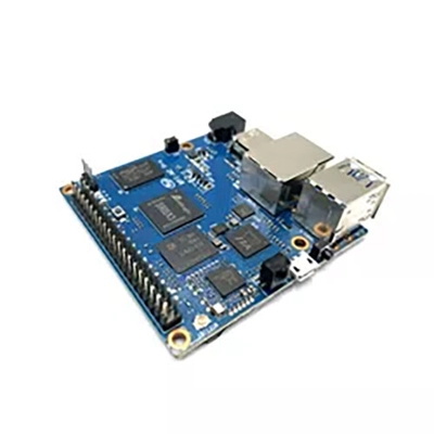
Introduce
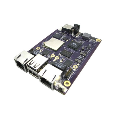
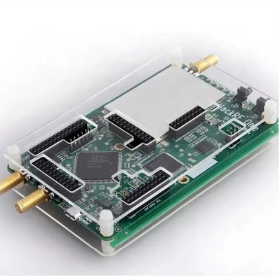
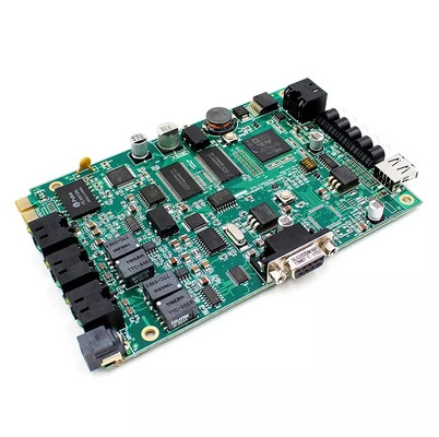
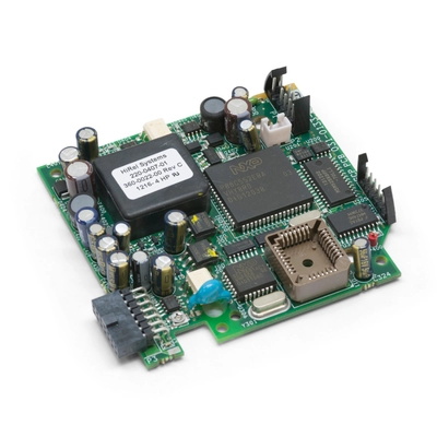
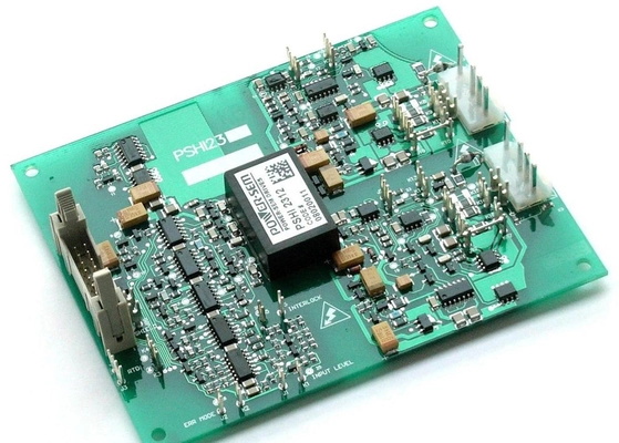
Zhiheng Xingsheng offers one-stop, full and partial turnkey PCB assembly services to meet all customer’s requirements and save time. Our quality-driven PCB assembly process ensures that your finished project is of the highest quality.
In full turnkey PCBA, we handle everything, including making circuit boards, ordering components, online order tracking, quality inspection and final assembly.
In partial turnkey PCBA, customers are responsible for supplying us the certain components, a partial list of parts, and the remaining parts. You can order the PCBs and partial components. We will fix the remaining parts, and manufacturing and assembly will be handled by us.